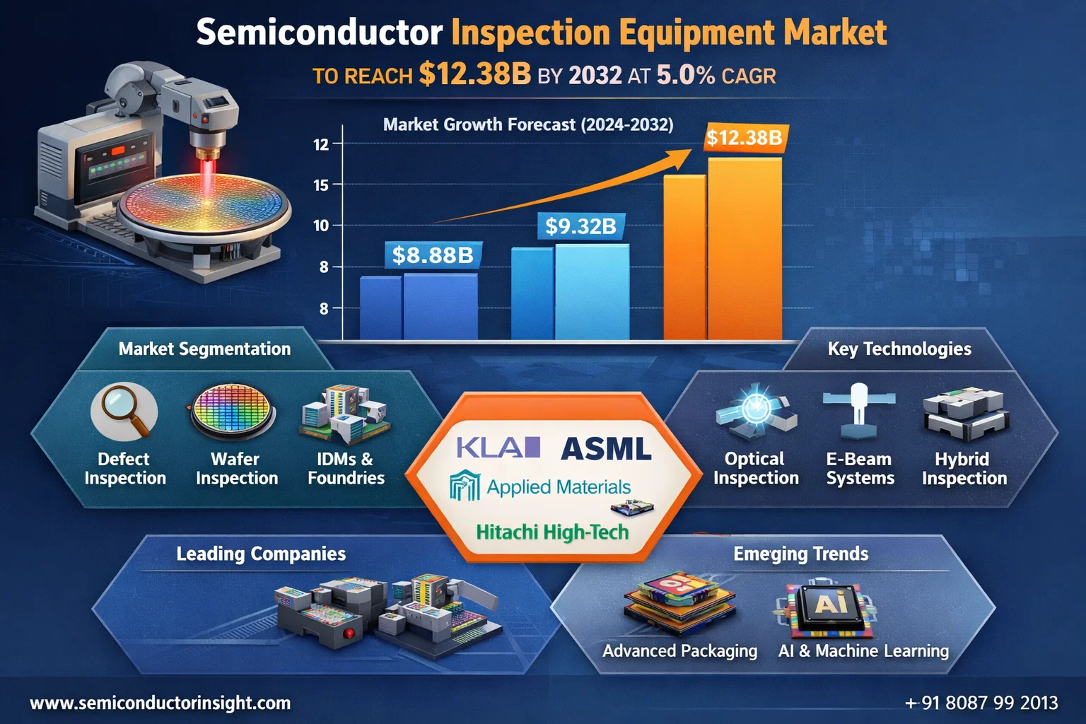
Semiconductor Inspection Equipment Market to Reach $12.38B by 2032 at 5.0% CAGR
The global Semiconductor Inspection Equipment Market was valued at USD 8,879 million in 2024 and is projected to grow to USD 12,380 million by 2032, expanding at a CAGR of 5.0%. The growth is driven by the increasing complexity of semiconductor manufacturing, shrinking chip geometries below 5nm, and the rising need for advanced inspection systems that can detect nanometer-scale defects during fabrication.
Inspection and metrology equipment play a crucial role in maintaining manufacturing yield, ensuring quality control, and enabling real-time process monitoring across hundreds of fabrication steps. As the industry advances toward 3D architectures, gate-all-around transistors, and advanced packaging technologies, the demand for hybrid inspection systems combining optical and e-beam technologies is increasing.
Additionally, the integration of artificial intelligence and machine learning in inspection tools is enhancing defect detection accuracy and enabling predictive maintenance. The Asia-Pacific region, which hosts the majority of global semiconductor manufacturing capacity, remains the dominant market for inspection equipment. Emerging opportunities in advanced packaging, compound semiconductors, and next-generation nodes such as 2nm and below are expected to further drive market growth in the coming years.
#Semiconductor #SemiconductorMarket #InspectionEquipment #SemiconductorManufacturing #ChipManufacturing #SemiconductorTechnology #WaferInspection #MetrologySystems #AdvancedPackaging #AIinSemiconductors #EBeamInspection #OpticalInspection #ChipIndustry #SemiconductorInnovation #ElectronicsManufacturing #TechMarketResearch #SemiconductorIndustry #ManufacturingTechnology #Nanotechnology #SemiconductorGrowth
Semiconductor Inspection Equipment Market to Reach $12.38B by 2032 at 5.0% CAGR
The global Semiconductor Inspection Equipment Market was valued at USD 8,879 million in 2024 and is projected to grow to USD 12,380 million by 2032, expanding at a CAGR of 5.0%. The growth is driven by the increasing complexity of semiconductor manufacturing, shrinking chip geometries below 5nm, and the rising need for advanced inspection systems that can detect nanometer-scale defects during fabrication.
Inspection and metrology equipment play a crucial role in maintaining manufacturing yield, ensuring quality control, and enabling real-time process monitoring across hundreds of fabrication steps. As the industry advances toward 3D architectures, gate-all-around transistors, and advanced packaging technologies, the demand for hybrid inspection systems combining optical and e-beam technologies is increasing.
Additionally, the integration of artificial intelligence and machine learning in inspection tools is enhancing defect detection accuracy and enabling predictive maintenance. The Asia-Pacific region, which hosts the majority of global semiconductor manufacturing capacity, remains the dominant market for inspection equipment. Emerging opportunities in advanced packaging, compound semiconductors, and next-generation nodes such as 2nm and below are expected to further drive market growth in the coming years.
#Semiconductor #SemiconductorMarket #InspectionEquipment #SemiconductorManufacturing #ChipManufacturing #SemiconductorTechnology #WaferInspection #MetrologySystems #AdvancedPackaging #AIinSemiconductors #EBeamInspection #OpticalInspection #ChipIndustry #SemiconductorInnovation #ElectronicsManufacturing #TechMarketResearch #SemiconductorIndustry #ManufacturingTechnology #Nanotechnology #SemiconductorGrowth
·14 Прегледи
·0 Осврти